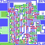
Integrated Circuit
 Today was a momentous occasion, as after a two weeks of long, hard work,
my IC design project came to a temporary conclusion. The conclusion is
temporary, because although the design is finalized, there is a
month-long fabrication process before students get to test their design
in real NMOS silicon. Then there is also the project report, which is
due soon thereafter.
Carleton has a small fabrication facility that can produce fairly simple chips. This project is NMOS simply because of the time constraints and the relative complexity of producing CMOS logic (several more masks and layers). Nevertheless, I find the entire process very exciting. The class associated with the project is definitely amongst my undergraduate favourites.
The chip design was permitted an area of 230λ by 230λ, where λ=2.5μm. This means that my whole project has an area of 5.75mm by 5.75mm. That would make it the smallest project I've ever completed. My tuny initials would only fit sideways in the bottom-right corner, and even then I couldn't close the "P" properly! My record for the longest time in a lab was reached today: I spent 11.5 hours with two 5 minute breaks finalizing this chip.
Edit (2005-12-14):
(230)(2.5μm) = 0.575mm. Thinking about this after the fact, the entire classes projects fit in an area smaller than 5mm by 5mm.
